Modern high-performance embedded systems and FPGAs demand lightning-fast memory access, but integrating Double Data Rate (DDR) memory can be a daunting challenge. The intricate timing requirements, pin assignments, and signal integrity considerations often transform what should be a straightforward task into a significant design hurdle. This is where the Memory Interface Generator (MIG) steps in, offering a powerful solution that abstracts away much of this complexity, allowing engineers to focus on the core innovation of their designs.
At its heart, MIG is more than just a tool; it's a vital bridge between complex memory standards and the robust capabilities of Xilinx FPGAs. By automating the creation of high-speed memory controllers, MIG empowers designers to achieve optimal performance without getting bogged down in the minute details of DDR interface design.
Unlocking High-Performance Memory Design
Imagine having a dedicated expert on DDR memory controller design right at your fingertips. That's essentially what MIG provides. Initially conceived in 2002 as a specialized pin selection utility, MIG has evolved into a sophisticated gateware and primitive instantiation generator supporting every Xilinx FPGA device, from the early Virtex-II to the latest UltraScale+ architectures. It dynamically produces all the necessary HDL (in Verilog or VHDL) and crucial constraints for high-performance operation. To truly grasp the foundational principles and capabilities of this essential tool, we encourage you to Explore Memory Interface Generators.
This evolution means that instead of spending countless hours poring over memory datasheets and constraint manuals, you can leverage MIG to automatically generate a tailored memory controller. The output is provided in non-encrypted, modifiable formats, offering full transparency and flexibility for further customization if needed.
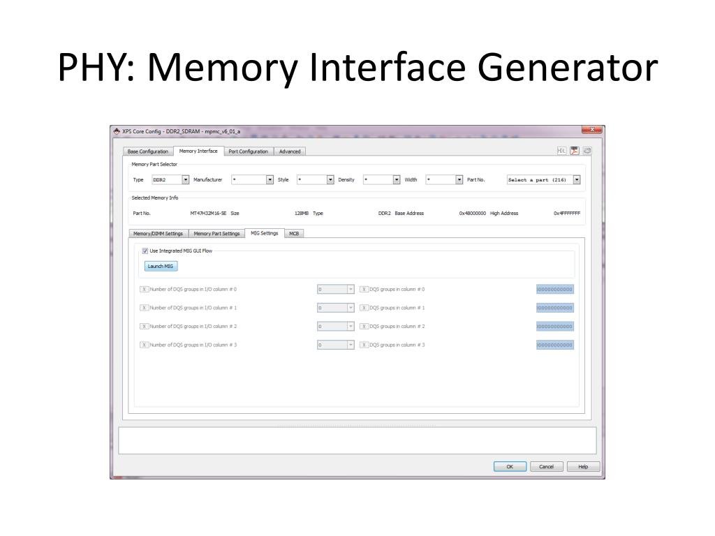
Navigating Memory Standards and Architectures
The world of DDR memory is rich with various standards—DDR3, DDR4, LPDDR4, and beyond—each with its own unique specifications and architectural nuances. Interfacing with these memories requires precise adherence to these standards, a task made significantly easier with MIG. It ensures that the generated controller is fully compliant, providing the necessary glue logic and timing to interact seamlessly with your chosen memory device.
Understanding the specific requirements of different memory types and how they integrate into various FPGA architectures is crucial for achieving peak system performance. MIG inherently handles these intricacies, allowing you to select your target memory and FPGA, then generate an optimized interface. Dive deeper into the diverse landscape of memory technologies and the underlying architectures they employ by choosing to Explore Memory Interface Standards & Architectures.
Streamlining Design and Integration Workflows
One of MIG's most significant contributions is its ability to streamline the entire design and integration process within the Vivado environment. Manual configuration of MIG parameters can be prone to errors and difficult to maintain across different Vivado and MIG versions. This is where advanced integration features come into play. Vivado Board Files, for instance, dramatically simplify the creation of memory interfaces by providing pre-configured MIG parameters for specific development boards.
Companies like Opal Kelly maintain detailed MIG configuration parameters within their Vivado Board Files for all their USB3 boards, making these readily available through AMD-Xilinx’s Board Store. This ensures seamless access to Vivado version-specific configurations, integrating directly into the Vivado GUI. Whether you're instantiating a DDR board component in IP Integrator (IPI) Project Mode or applying parameters via a TCL scripting command, MIG simplifies this critical step for supported modules like the Artix UltraScale+ (XEM8310, XEM8320) or Kintex-7 (XEM7350, XEM7360). For a comprehensive look at how to effectively incorporate MIG into your project, be sure to Explore Design & Integration Workflows.
Ensuring Robustness Through Verification and Validation
Generating a memory interface is just the first step; ensuring its robustness and reliability is paramount. MIG doesn't just output HDL; it also generates critical constraints like .ucf pin constraints, and slice and logic placement constraints, all designed to facilitate high-performance operation. However, even with automated generation, thorough verification and validation of the generated IP are essential.
This involves simulating the memory controller, testing its functionality on hardware, and ensuring it meets all performance targets. Since MIG's outputs are modifiable, designers have the flexibility to inspect and fine-tune the generated code and constraints, though careful validation is always required after any manual adjustments. To learn how to thoroughly test and confirm the functionality of your generated memory interface, we recommend you delve into Verification & Validation of Generated.
Mastering Performance, Power, and Area (PPA) Optimization
In high-speed digital design, the triumvirate of Performance, Power, and Area (PPA) dictates the success of any system. A memory interface must not only be functional but also optimized to meet stringent PPA targets. MIG plays a crucial role here by generating optimized HDL and precise constraints that guide the Vivado implementation tools to achieve the best possible PPA for the memory controller.
These constraints ensure proper timing closure, minimize power consumption, and optimize the utilization of FPGA resources, which is especially critical for complex designs leveraging 7-Series and UltraScale FPGAs. Achieving a balance between these factors often requires a deep understanding of the underlying FPGA architecture and the memory controller's operational characteristics. Discover the techniques and considerations for fine-tuning your memory interface to achieve optimal PPA by exploring Performance, Power, and Area (PPA.
As embedded systems continue to push the boundaries of data throughput and processing, the role of tools like the Memory Interface Generator will only grow more critical. It simplifies the inherently complex task of integrating high-speed memory, allowing innovators to focus on their next breakthrough, rather than getting entangled in low-level interface details. The future of high-performance FPGA design will undoubtedly continue to rely on such sophisticated automation to unlock new possibilities.