The heartbeat of every electronic device, from the smartphone in your pocket to the powerful AI accelerators driving innovation, is a silicon chip. But what makes one chip a marvel of engineering and another a forgotten prototype? Often, it boils down to the delicate, complex dance of Performance, Power, and Area (PPA) Optimization. This isn't just a technical challenge; it's the very soul of modern VLSI design, a continuous tug-of-war between competing demands to deliver chips that are fast, energy-efficient, and compact.
For chip designers, balancing PPA isn't just about ticking boxes; it's about crafting the optimal trade-off for a specific application, much like a master chef balances flavors for the perfect dish. Push for extreme speed, and you might drain batteries in minutes. Shrink the size too much, and manufacturing costs could skyrocket, or performance could suffer. This article unpacks the critical PPA optimization challenge, exploring its core components, the intricate trade-offs involved, and the sophisticated techniques used to master them across the chip design lifecycle.
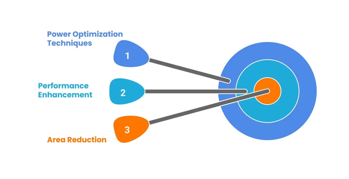
At a Glance: Key Takeaways on PPA Optimization
- PPA Defined: PPA stands for Performance (speed), Power (energy consumption), and Area (silicon size). These are the three pillars of chip design.
- The Golden Triangle: Improving one PPA metric almost always negatively impacts another. Optimization is about finding the right balance for the chip's intended use.
- Power is Paramount: Essential for battery-powered devices (smartphones, IoT) and thermal-sensitive systems (AI servers).
- Performance is Speed: Measured by clock frequency, throughput, and latency; defines how fast a chip gets work done.
- Area is Cost: Directly impacts manufacturing costs and yield, especially for high-volume chips.
- Optimization is Iterative: PPA decisions are made and refined at every stage of design, from initial RTL coding to final physical layout.
- Holistic Approach: True PPA mastery requires a deep understanding of how choices at one stage ripple through the entire design flow.
The Golden Triangle: Defining Performance, Power, and Area
Before we dive into the optimization strategies, let's establish a clear understanding of each leg of the PPA triangle. Each metric holds unique significance and presents its own set of challenges.
Performance: The Need for Speed
Performance, at its core, is about how quickly and efficiently a chip can execute its tasks. Think of it as the chip's athleticism—how fast it can run, how many computations it can complete per second, and how quickly it responds to commands.
- Key Metrics:
- Clock Frequency (GHz): The speed at which the chip's internal clock oscillates, driving synchronous operations. A higher frequency generally means more operations per second.
- Throughput: The total amount of work completed over a given time. For instance, how many frames per second a GPU can render, or how many network packets an SoC can process.
- Latency: The delay between an input and the corresponding output. Lower latency is crucial for real-time applications where quick responses are critical.
- Influencing Factors:
- Critical Path Delay: The longest combinational path in a circuit. This path determines the maximum clock frequency at which the chip can reliably operate.
- Clock Tree Synthesis (CTS) and Skew: The distribution network for the clock signal. An optimized clock tree ensures the clock arrives at all flip-flops simultaneously, minimizing skew (differences in arrival times) which can eat into timing margins.
- Pipeline Depth: Dividing complex operations into smaller stages executed sequentially. Deeper pipelines can increase throughput but might also increase latency.
- The Goal: Maximize the operating frequency and throughput while ensuring all timing constraints are met, without introducing glitches or signal integrity issues.
Power: The Energy Equation
Power refers to the electrical energy consumed by the chip. In an increasingly mobile and environmentally conscious world, power consumption is no longer a secondary concern; it's often the primary design driver for many applications.
- Types of Power Consumption:
- Dynamic Power: The dominant power type in many active circuits, caused by the switching activity of transistors (charging and discharging capacitances). It's directly proportional to frequency, capacitance, and the square of the voltage ($P_{dynamic} \propto C \cdot V^2 \cdot f$).
- Static Power (Leakage Power): Power consumed when transistors are idle (not switching). Even when circuits aren't actively doing work, a small leakage current flows. As process technologies shrink, static power becomes an increasingly significant challenge.
- Short-Circuit Power: A momentary current draw during the brief period when both the PMOS and NMOS transistors in a CMOS gate are simultaneously on during a logic transition, creating a temporary path from power to ground.
- Why it's Critical: For battery-operated devices, low power extends battery life. For high-performance chips (like those in data centers), excessive power means more heat, requiring elaborate and expensive cooling solutions, or leading to thermal throttling which limits performance.
- The Goal: Reduce overall power consumption without unduly sacrificing performance or requiring excessive area.
Area: The Silicon Footprint
Area refers to the physical silicon real estate occupied by the chip's logic gates, memory blocks, and interconnects. It's often measured in square millimeters (mm²).
- Impact of Area:
- Fabrication Cost: Larger chips mean fewer chips per silicon wafer, directly increasing the cost per chip. In high-volume manufacturing, even a small reduction in area can save millions.
- Yield: Smaller chips generally have higher manufacturing yield, as they are less likely to contain defects that render a larger chip unusable.
- Power Consumption: Larger area can lead to longer interconnects between components, increasing wire capacitance and thus dynamic power consumption.
- Optimization Strategies:
- Gate-Level Optimization: During synthesis, choosing smaller, more efficient standard cells to implement logic.
- Resource Sharing in RTL: Designing RTL code to reuse functional blocks (e.g., a single multiplier instead of multiple dedicated ones if timing allows).
- Efficient Standard Cell Usage: Selecting the right library cells for each function to balance speed and size.
- Floorplanning: Strategically arranging large functional blocks (IP cores, memory banks, custom logic) early in physical design to minimize wire lengths and improve overall layout.
- The Goal: Achieve maximum functionality and performance within the minimum possible die size, while respecting power and timing constraints.
The Inevitable Dance: Understanding PPA Trade-Offs
Here's the fundamental truth of chip design: PPA metrics are almost always in conflict. You pull one lever, and another metric shifts, often in an undesirable direction. This is why PPA optimization is less about achieving absolute maxima for each and more about finding the optimal balance for the specific application.
Let's look at some common trade-offs:
- Performance vs. Power: To increase performance, you might need a higher clock frequency. Higher frequency directly translates to higher dynamic power consumption. Alternatively, using faster (but often larger and leakier) standard cells to meet timing means more static power.
- Area vs. Performance: Reducing area often means packing more logic into a smaller space. This can lead to routing congestion, making it harder to connect all components efficiently. Longer or more tortuous interconnects due to congestion increase signal delays, potentially degrading performance and making it harder to meet timing.
- Power vs. Area: Techniques to reduce power, such as using multi-Vt cells (e.g., slower, low-leakage High Vt cells), might require larger transistors or more complex power-gating structures, thus increasing area. Conversely, very small, dense designs can lead to thermal hot spots, increasing leakage power.
- Area vs. Power (Again): While reducing area can sometimes increase power (due to higher density and leakage), larger interconnects in a sprawling design also contribute to dynamic power. The ideal is often a compact, well-planned layout that minimizes both active and passive power.
This intricate interplay means PPA optimization isn't a one-and-done task. It's a continuous, iterative process involving tweaks and analyses at every stage of the design flow, from initial RTL architectural decisions to the final physical layout. Each change necessitates re-evaluation of its impact across all three PPA dimensions.
Optimizing PPA: Strategies Across the Design Flow
Achieving PPA targets requires a holistic approach, starting from the very first line of code and extending through the intricate stages of physical layout. Each design stage offers unique opportunities to influence performance, power, and area.
From Concept to Silicon: How PPA is Shaped at Each Stage
1. RTL Design (Register-Transfer Level)
This is where the chip's functional behavior is described using hardware description languages (like Verilog or VHDL). Early architectural decisions here have the most profound PPA impact.
- Efficient Coding: Writing clean, optimized RTL that avoids redundant logic, unnecessary registers, or complex combinational paths.
- Finite State Machine (FSM) Optimization: Designing FSMs with minimal states and efficient transitions can reduce logic complexity and critical path delay.
- Resource Sharing: Reusing a single hardware block (like an adder or multiplier) for multiple operations across different clock cycles, rather than duplicating the block, can significantly reduce area (at the potential cost of some performance/latency).
- Pipelining: Breaking down long combinational paths into smaller, sequential stages to allow for higher clock frequencies, boosting performance.
- Low-Power RTL Coding: Implementing techniques like clock gating at the RTL level, where clock signals to idle blocks are stopped, drastically reducing dynamic power.
2. Logic Synthesis
Synthesis translates the abstract RTL description into a gate-level netlist, mapping the logic to specific standard cells from a technology library.
- Gate-Level Optimization: Synthesis tools analyze the netlist and select the most appropriate standard cells (e.g., inverters, NAND gates, flip-flops) to meet PPA targets. This includes logic restructuring and technology mapping.
- Multi-Vt Cell Usage: Leveraging different threshold voltage (Vt) cells.
- High-Vt (HVT) / Regular-Vt (RVT): Slower, lower leakage power, used for non-critical paths or areas where power is paramount.
- Low-Vt (LVT) / Super Low-Vt (SLVT): Faster, higher leakage power, used for critical paths to meet timing.
- This technique allows designers to selectively use faster cells only where absolutely necessary, saving power and area elsewhere.
3. Physical Design (Place & Route)
This is where the logical netlist is transformed into the physical layout of the chip on silicon. This stage is crucial for realizing the PPA goals set earlier.
- Floorplanning: Strategically arranging major functional blocks (cores, memories, I/Os) on the die. A good floorplan minimizes interconnect lengths (reducing dynamic power and delay), prevents routing congestion, and facilitates power distribution.
- Placement: Arranging individual standard cells and macros within the floorplan. Optimized placement ensures:
- Neat Wiring & Short Distances: Cells that communicate frequently are placed close together, minimizing wire length.
- Small Delay: Shorter wires mean less parasitic capacitance and resistance, leading to faster signal propagation.
- Reasonable Device Layout: Spreading out power-hungry blocks to avoid hot spots, or grouping low-power blocks together.
- Clock Tree Synthesis (CTS): Building a balanced clock distribution network to deliver the clock signal to all clocked elements with minimal skew and insertion delay. A well-built clock tree is vital for meeting performance targets.
- Routing Optimization: Connecting all the placed cells with metal wires. Advanced routers strive to:
- High Density, Small Area: Use minimal routing resources while maintaining signal integrity.
- Low Power: Minimize wire length to reduce dynamic power.
- Meet Timing: Route critical paths optimally to minimize delay.
- Power Gating: Strategically turning off power to idle blocks or entire sections of the chip during periods of inactivity to eliminate both dynamic and static power consumption in those regions.
4. Static Timing Analysis (STA) & Signoff
STA is a comprehensive analysis performed throughout the design flow to verify that all timing constraints are met. Signoff is the final stamp of approval before fabrication.
- Timing Closure: Iteratively refining the design (often through placement and routing adjustments or small logical changes) until all timing paths meet their requirements (i.e., no negative slack).
- Slack Analysis: Identifying critical paths (paths with minimal positive or negative slack) and focusing optimization efforts there.
- Engineering Change Order (ECO) Fixing: Small, localized changes to the netlist or layout to fix timing violations or other issues late in the design cycle.
5. Post-Silicon Validation & Optimization
Even after the chip is fabricated, there are still opportunities for PPA optimization.
- Dynamic Voltage Frequency Scaling (DVFS): Adjusting the operating voltage and frequency of different chip blocks in real-time based on workload. This is a powerful technique for reducing dynamic power: when less performance is needed, voltage and frequency can be lowered significantly, saving considerable energy ($P_{dynamic} \propto V^2 \cdot f$). This is often managed by specialized control units and can respond to commands, for instance, from a PMBUS-controlled power management IC.
- Thermal Throttling: Reducing clock frequency and/or voltage when the chip's temperature exceeds a predefined threshold to prevent damage and manage power.
If you're delving into the intricacies of system-level performance, understanding how different components communicate is key. For example, effectively managing data flow to and from memory is critical, and you might want to Learn about memory interface generators for optimizing these crucial connections.
Deep Dive: Key PPA Optimization Techniques
Let's expand on some of the most impactful techniques mentioned above.
Power Reduction Techniques
- Clock Gating: A fundamental low-power technique where the clock signal to registers or entire functional blocks is conditionally disabled when they are not in use. This prevents unnecessary switching activity, significantly reducing dynamic power.
- Power Gating: More aggressive than clock gating, power gating completely cuts off the power supply to inactive blocks using header or footer switches (MOSFETs). This virtually eliminates both dynamic and static power in the gated region, making it ideal for blocks that can be powered down for extended periods.
- Multi-Vt Cells (HVT/RVT/LVT/SLVT): As discussed, using a mix of standard cells with different threshold voltages to balance speed and leakage power. Critical paths use faster, leakier LVT cells, while non-critical paths use slower, low-leakage HVT cells.
- Dynamic Voltage Frequency Scaling (DVFS): An operating system or hardware-controlled technique that dynamically adjusts the supply voltage and clock frequency of a chip or individual cores based on the current workload. High workload = high voltage/frequency; low workload = low voltage/frequency, saving substantial power. This often involves specialized power management ICs (PMICs) and communication protocols like PMBUS.
- Multi-Voltage Power Supply Technology: Employing multiple independent voltage domains on a single chip. Different domains can operate at different voltages tailored to their performance requirements (e.g., a high-performance core at 1.0V and a low-power peripheral at 0.8V).
- Low-Power RTL Coding: Designing RTL with an awareness of power. This includes avoiding unnecessary state changes, using efficient arithmetic structures, and incorporating explicit clock-gating conditions.
Performance Maximization Techniques
- Critical Path Analysis and Optimization: Identifying the longest delay path in the circuit (the critical path) and applying various techniques to shorten it. This might involve logic restructuring, using faster standard cells, or buffering to reduce fanout.
- Clock Tree Synthesis (CTS) and Skew Optimization: Designing a clock distribution network that ensures the clock signal arrives at all sequential elements with minimal differences in arrival time (skew). Low skew allows for higher clock frequencies.
- Pipelining: Breaking down complex operations into a series of smaller, sequential stages. This increases the total throughput by allowing multiple operations to be in flight simultaneously, even if the latency of a single operation might increase.
- Advanced Static Timing Analysis (STA): Using sophisticated STA tools to accurately model and verify timing, considering variations in process, voltage, and temperature (PVT variations), to ensure robust operation at target frequencies.
Area Reduction Techniques
- Gate-Level Optimization during Synthesis: Synthesis tools can perform logic minimization and technology mapping to implement the desired functionality with the smallest possible number of standard cells, or the most compact cells available in the library.
- Resource Sharing in RTL: Design at the RTL level to reuse hardware blocks. For example, if two operations happen at different times, they might share a single adder instead of each having their own. This can be a performance/area trade-off.
- Efficient Standard Cell Usage: Careful selection of standard cells. Sometimes, a complex gate (e.g., an AOI - AND-OR-Invert gate) can implement a function more compactly than using multiple basic gates.
- Effective Floorplanning and Placement: A well-thought-out floorplan groups related logic, minimizes routing congestion, and reduces the need for large buffer cells to drive long interconnects, all contributing to a smaller final die size.
Real-World Impact: Why PPA Matters for Every Chip
The relative importance of Performance, Power, and Area shifts dramatically depending on the chip's end application. Understanding these priorities is key to successful PPA optimization.
- Smartphone SoCs: Power is often the primary driver (battery life), followed by Performance (smooth user experience) and then Area (compact device form factor). Optimizations like DVFS, aggressive clock/power gating, and multi-voltage domains are critical here.
- AI Accelerators (Data Center): Performance (raw computational throughput for neural networks) is usually paramount, followed by managing Power (due to massive scale and cooling costs), with Area being less critical unless it impacts cost per wafer excessively. Designers might use highly parallel architectures and focus on efficient data flow.
- IoT Sensor Chips: Power is overwhelmingly the most critical factor (multi-year battery life for remote sensors), with Area (tiny form factor) and minimal Performance (simple data collection) following. Ultra-low power design techniques, extreme power gating, and always-on, low-leakage logic are essential.
For anyone pursuing a career in the semiconductor industry, a deep understanding of PPA is fundamental. Common interview questions often probe your knowledge of how to reduce dynamic power, the relationship between timing slack and performance, or how physical placement decisions impact both area and power consumption. The ability to articulate these trade-offs and propose solutions is a hallmark of a proficient chip designer.
Beyond the Metrics: The Future of PPA
As semiconductor technology continues to push the boundaries of physics, PPA optimization faces ever-evolving challenges. Advanced process nodes (e.g., 3nm, 2nm) bring increased transistor density, but also greater leakage power and more complex variability issues. Emerging architectures like chiplets, 3D stacking, and in-memory computing introduce new ways to manage power and performance at a system level, while also presenting novel integration and thermal challenges.
The drive for sustainable computing, the explosion of AI at the edge, and the demand for increasingly powerful yet portable devices ensure that PPA optimization will remain at the forefront of innovation for decades to come.
Your PPA Journey: Mastering the Art of Balance
PPA optimization isn't a science with a single right answer; it's an art of balance, a continuous negotiation between competing forces. It demands a holistic view, an understanding of the entire chip design flow, and the courage to make tough trade-offs.
Whether you're an aspiring chip designer, an engineer looking to deepen your expertise, or simply curious about the magic behind modern electronics, grasping the principles of Performance, Power, and Area optimization is key. It's about more than just numbers; it's about shaping the future of technology, one incredibly optimized chip at a time. The journey requires continuous learning, robust tools, and a keen eye for how every decision—big or small—ultimately impacts the final product. Dive in, experiment, and keep asking how you can make it faster, cooler, and smaller.