The insatiable appetite for data in modern computing has pushed traditional system architectures to their limits. Processors have become incredibly powerful, but their true potential is often bottlenecked by one critical factor: how quickly and efficiently they can access memory. For many systems, the real challenge isn't processing speed, but the speed of data movement. This is where Understanding Memory Interface Generators becomes not just important, but essential for unlocking next-generation performance and efficiency.
Imagine a superhighway connecting your city's busiest districts. If that highway is narrow, riddled with tolls, and constantly under construction, even the fastest cars will crawl. In computing, that highway is the memory interface—the conduit between your processing units and the vast oceans of data stored in RAM, flash, and other memory types. For too long, designers have cobbled together generic interfaces, leading to performance compromises. Now, a sophisticated solution has emerged, one that custom-builds that highway for peak efficiency: the Memory Interface Generator (MIG).
At a Glance: Why Memory Interface Generators Matter
- Customized Performance: MIGs generate tailor-made memory interfaces, optimizing data transfer rates for your specific application.
- Latency Slasher: By streamlining data pathways, they significantly reduce the time it takes for your processor to fetch data.
- Power Saver: Optimized interfaces mean less energy wasted on data movement, crucial for power-sensitive devices.
- Future-Proof Flexibility: MIGs can scale and adapt to evolving memory technologies and application demands.
- Crucial for AI & Data Centers: They are vital for powering high-performance, data-intensive workloads in AI, edge computing, and large-scale data centers.
What Exactly is a Memory Interface Generator (MIG)?
At its core, a Memory Interface Generator (MIG) is a sophisticated tool or IP (Intellectual Property) block that designs and implements the communication link between your system's processing logic and its memory components. Think of it as a specialized architect and engineer rolled into one, meticulously crafting the ideal bridge for data.
Historically, interfacing with memory—especially complex, high-speed DRAM—was a daunting task. It required deep expertise in electrical engineering, timing analysis, and controller logic design. Designers had to manually configure timing parameters, impedance matching, signal integrity, and a myriad of other subtle factors to ensure reliable operation. This manual approach was prone to errors, time-consuming, and rarely yielded truly optimal performance.
The MIG changes this paradigm. It takes your application's specific requirements—data types, processing speed, desired memory capacity, power constraints—and uses advanced algorithms, sometimes even incorporating machine learning techniques, to generate a highly customized and optimized memory interface. This isn't just a generic template; it's a bespoke solution designed to maximize data transfer rates, minimize latency, and reduce power consumption for your unique system.
The resulting interface typically manifests as a combination of hardware and software:
- Hardware: Often implemented within Field-Programmable Gate Arrays (FPGAs) or Application-Specific Integrated Circuits (ASICs), where dedicated I/O blocks and logic gates are configured.
- Software: Includes the embedded memory controller logic that manages access, refresh, and data flow.
The Indisputable Benefits of a Smartly Designed Memory Interface
Leveraging a MIG offers compelling advantages that ripple through your entire system's performance profile:
- Improved Performance: By optimizing every aspect of the data path, MIGs can dramatically accelerate data transfer rates. This means your CPU or specialized accelerator spends less time waiting for data, directly translating to faster processing and higher throughput for your applications.
- Reduced Latency: Latency—the delay between a request for data and its arrival—is often the silent killer of system responsiveness. A MIG meticulously tunes signal paths and timing parameters to slash data transfer latency, making systems feel snappier and more reactive, critical for real-time applications.
- Increased Efficiency: Unoptimized memory interfaces can consume significant power, especially at high speeds. MIGs are designed to reduce this overhead, making them invaluable for energy-constrained devices like mobile electronics, edge devices, and large-scale data centers looking to minimize their carbon footprint.
- Enhanced Scalability: As your application needs evolve, a well-designed MIG offers the flexibility to scale. Whether you need to increase memory capacity, boost bandwidth, or adapt to new memory standards, the underlying architecture generated by a MIG is typically more adaptable than a hand-coded, rigid solution.
The Crucial Role of the Memory Interface Itself
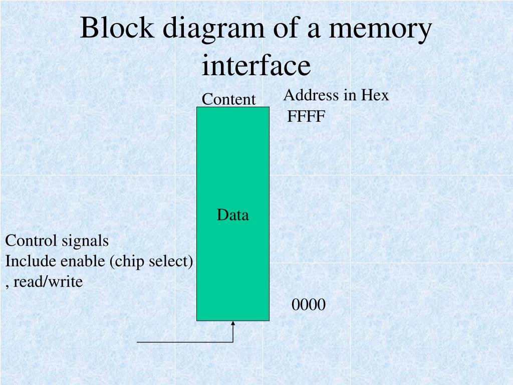
Before we dive deeper into MIGs, it's essential to grasp the fundamentals of the memory interface they generate. A memory interface is the essential physical and logical structure that connects your computer system's processing units (like a CPU, GPU, or FPGA) to various types of memory, be it RAM, Flash, or DRAM. It's the critical bridge that facilitates the bidirectional transfer of data, instructions, and control signals.
Understanding the Core Signals
Every memory interface relies on a set of standardized signals to communicate:
- Clock: Synchronizes operations between the processor and memory.
- Data Bus: Carries the actual information being read from or written to memory. Its width (e.g., 8-bit, 32-bit, 64-bit) determines how many bits can be transferred simultaneously.
- Address Bus: Specifies the exact location in memory where data needs to be accessed.
- Read/Write Controls: Signals that tell the memory whether the processor wants to retrieve data (read) or store new data (write).
These signals are meticulously defined in hardware description languages (HDLs) like VHDL and Verilog during the design phase. An efficient memory interface isn't just about having these signals; it's about optimizing their timing, voltage levels, and physical routing to achieve maximum performance and reliability. Bandwidth (how much data can be transferred per unit of time) and latency directly dictate how quickly a CPU can access and process information.
Parallel vs. Serial: Different Roads for Data
Memory interfaces are broadly categorized by how they transmit data:
- Parallel Interfaces: These interfaces transfer all data bits simultaneously, requiring a separate wire for each bit, address line, and control signal.
- Pros: Offer very high speed, capable of byte or even word transfers in microseconds or nanoseconds. This direct, wide pathway is fantastic for raw throughput.
- Cons: Require many pins and wires, leading to larger circuit sizes and more complex, expensive printed circuit board (PCB) layouts.
- Example: Traditional DRAM interfaces, where a 64-bit data bus would literally have 64 data lines.
- Serial Interfaces: These interfaces transfer data bits one after another over a smaller number of wires.
- Pros: Significantly reduce pin count and circuit size, making them ideal for smaller form factors or connecting to large data storage with fewer physical connections.
- Cons: Generally slower than parallel interfaces for the same clock frequency, though advancements have made high-speed serial links incredibly performant.
- Examples: I2C (Inter-Integrated Circuit) and SPI (Serial Peripheral Interface) are common for slower peripherals or non-volatile memory like Flash/EEPROM. SPI, for instance, uses four wires (serial data in, serial data out, clock, chip select) and supports full-duplex communication, making it prevalent for flash memory.
Volatile vs. Nonvolatile: Memory with a Purpose
The type of memory being interfaced also dictates specific design considerations:
- Volatile Memory Interfaces: These connect to system memory like DRAM (Dynamic Random Access Memory), which requires constant power and periodic "refresh" cycles to retain data. Data is lost when power is removed.
- Purpose: Primarily used for working memory where speed and temporary storage are paramount.
- Example: The interface for your computer's main RAM.
- Nonvolatile Memory Interfaces: These connect to storage devices like Flash memory or EEPROM (Electrically Erasable Programmable Read-Only Memory), which retain data even without power.
- Purpose: Used for persistent storage of operating systems, applications, and user data.
- Example: The interface to your SSD or a microcontroller's program memory.
The choice between these depends critically on requirements for speed, capacity, and data retention.
A Deep Dive into DRAM and Its Interfaces
DRAM is the workhorse of volatile system memory, and its interface design has undergone continuous evolution to meet escalating demands. DRAM is internally organized into banks, rows, and columns. Accessing data involves a precise sequence of activate, read, or write commands, all while juggling the need for periodic refresh cycles to prevent data loss.
The Evolution of DRAM Interfaces
- SDRAM (Synchronous DRAM): A significant leap from asynchronous DRAM, SDRAM synchronized its operations with the system clock, allowing for more predictable and faster data transfers.
- DDR SDRAM (Double Data Rate): This innovation truly revolutionized memory performance. DDR transfers data on both the rising and falling edges of the clock signal, effectively doubling the data rate without increasing the clock frequency.
- DDR2: Further increased bus clock speeds and introduced 4n-prefetch architecture, meaning it could fetch four 64-bit words for every clock cycle on the memory array.
- DDR3: Elevated performance again, operating the bus clock at four times the internal memory clock frequency, utilizing an 8n-prefetch architecture to fetch eight 64-bit words per cycle. This constant drive to prefetch more data per cycle is a key strategy for boosting effective bandwidth.
The standardization of DRAM and memory modules is largely driven by the JEDEC Solid-State Technology Association, ensuring interoperability and consistent performance across the industry.
Memory Modules: From SIMMs to SO-DIMMs
The physical packaging of DRAM chips has also evolved to support denser, higher-performance interfaces:
- SIMMs (Single In-line Memory Modules): Early modules with typically 8- or 9-bit data buses.
- DIMMs (Dual In-line Memory Modules): The standard for modern desktop and server PCs, supporting wider 64- or 72-bit interfaces for much denser signal routing and higher capacity.
- SO-DIMMs (Small Outline DIMMs): Smaller, compact versions of DIMMs, standardized for mobile devices and laptops.
These modules house multiple DRAM chips and provide the standardized electrical interface to the motherboard.
Navigating the Complexities: Challenges in High-Performance Interface Design
Designing a high-performance parallel memory interface, even with the aid of a MIG, presents significant challenges:
- Achieving High Bandwidth: Pushing data rates ever higher demands meticulous attention to signal integrity, noise reduction, and impedance matching across many parallel lines.
- Source-Synchronous Interfaces: For reliable high-speed data transfer, especially in parallel interfaces, a clock signal is often transmitted along with the data. This "source-synchronous" clock allows the receiving device to accurately sample the data at the correct moment, overcoming delays and skew. Precisely aligning this clock with the data is critical.
- Tight Timing Requirements: As frequencies increase, the window for correctly sampling data shrinks to picoseconds. Factors like clock jitter (variations in clock timing) and data bus skew (differences in arrival times for bits on the same bus) can quickly derail performance and reliability.
- FPGA I/O Blocks: Modern FPGAs offer specialized I/O (Input/Output) blocks with features like programmable delay lines, impedance calibration, and dedicated memory interface logic to help manage these tight timing requirements and achieve precise clock-to-data centering. A MIG leverages these features extensively.
Beyond the Wires: Memory Controllers and Software Management
While the physical interface defines the data highway, the memory controller is the traffic cop and dispatcher, orchestrating all memory operations. It's a highly optimized architecture designed to accommodate various factors:
- Bank Number: Manages multiple independent memory banks for parallel access.
- Bus Width & Device Width: Configures itself to match the physical interface.
- Access Algorithms: Implements strategies like page closing/opening, refresh cycles, and command scheduling to maximize efficiency and minimize latency.
The memory controller's primary role is to translate the processor's logical addresses into the physical bank, row, and column addresses required by the DRAM chips.
The Hardware-Software Synergy
Memory interfaces aren't purely hardware; they rely heavily on software components to function optimally:
- Device Drivers: These act as the software interface between the memory hardware and the operating system (OS). They abstract away complex hardware details, manage access privileges, and enable powerful features like Direct Memory Access (DMA), which allows peripherals to transfer data directly to/from memory without involving the CPU, freeing up the processor for other tasks.
- Memory Management Units (MMUs): These hardware components, often integrated into the CPU or memory controller, facilitate address translation. They convert virtual addresses used by software into physical addresses used by hardware, enabling crucial concepts like:
- Virtual Memory: Allows a system to use more memory than is physically installed, swapping data between RAM and storage.
- Page Tables: Data structures used by the MMU to map virtual pages to physical frames.
- Unified Virtual Memory (UVM): In modern heterogeneous computing platforms (e.g., systems with CPUs and GPUs), UVM allows seamless sharing of pointers and data structures between different processing units, simplifying programming and data management.
Software mechanisms also play a significant role in configuring and optimizing memory interfaces dynamically. This includes memory allocation strategies, address mapping (often using Translation Lookaside Buffers (TLBs) and Region Access Banks (RABs) for faster lookups), and power management routines that optimize access patterns and even restructure code to reduce memory-related energy consumption.
Redefining the Architecture: Processing-in-Memory & Emerging Technologies
The conventional computing model, where the CPU is separated from main memory, faces an increasingly severe problem: the "memory wall." Data transfers between the CPU and memory are costly in terms of both latency and energy. This bottleneck has spurred the development of revolutionary architectures and new memory technologies.
Processing-in-Memory (PIM) and Processing Near Memory (PNM)
These architectures aim to drastically reduce data movement by bringing computation closer to where the data resides.
- PIM: Integrates processing capabilities directly within the memory chips.
- PNM: Places specialized processing units very close to memory modules, minimizing the physical distance data has to travel.
These approaches promise substantial gains in energy efficiency and performance for memory-bound operations, particularly in AI and big data analytics. However, they require new software stacks, including runtime libraries and device drivers, to manage memory-bound operations, buffer allocation, and instruction generation effectively. Challenges include managing communication across different memory modules and the nascent maturity of some underlying technologies like memristors, which face issues with precision, ADC/DAC overheads, and durability.
High-Bandwidth Memory (HBM) and Hybrid Memory Cube (HMC)
These are prime examples of advanced memory interfaces designed to break the memory wall:
- HBM (High-Bandwidth Memory): Utilizes Through-Silicon Vias (TSVs)—vertical electrical connections that pass through the silicon die—to stack multiple DRAM dies directly on top of each other. This dramatically reduces the distance between the CPU/GPU and memory, resulting in significantly increased bandwidth and reduced power consumption. HBM is prevalent in high-performance GPUs and AI accelerators.
- HMC (Hybrid Memory Cube): Integrates both a logic layer (memory controller) and multiple stacked DRAM dies on a silicon substrate. It offers incredibly high transfer rates (up to 1 TBps) and supports vast amounts of memory.
These technologies enable higher system-level integration and unprecedented performance levels by directly addressing the physical distance and parallel access limitations of traditional memory architectures.
The Future is Heterogeneous and Disaggregated
The evolution of memory interfaces is increasingly marked by heterogeneity and a move towards disaggregated memory pools. New interconnects are paving the way:
- Open Memory Interface (OMI): An open standard designed to connect various memory types (DRAM, HBM, NVDIMMs) to processors.
- Computer Express Link (CXL): A high-speed interconnect that allows CPUs to seamlessly access memory in DDR slots alongside CXL Memory Expander devices in PCIe slots. CXL offers low latency (100–200 nanoseconds) and high bandwidth (up to 64 GB/s for 16 PCIe Gen5 lanes), enabling flexible memory expansion and resource pooling.
- NVDIMM (Non-Volatile DIMM): Combines traditional DRAM with non-volatile memory (like Flash) on a single module, providing persistent data storage at near-DRAM speeds. This is critical for data integrity in environments where power loss is a concern.
Looking further ahead, memory interfaces may adopt advanced SerDes (Serializer/Deserializer) technology, similar to what's used in 100 Gigabit Ethernet, pushing speeds to 25 Gbps per lane and significantly reducing pin count. This could even lead to industry-standard optical cabling for memory pools deployed separately from servers, allowing for truly disaggregated and composable memory architectures.
Choosing the Right MIG: Practical Considerations for Your System
Selecting and implementing the right Memory Interface Generator isn't a "set it and forget it" task. It requires careful consideration of your application's unique demands and system constraints.
Key Decision Criteria:
- Application Profile:
- Data Type & Access Patterns: Is your application performing large sequential reads (e.g., video streaming) or small, random accesses (e.g., database lookups)? A MIG can be tuned for burst efficiency or low-latency individual transactions.
- Throughput vs. Latency: Does your application prioritize maximum data volume (throughput) or minimal delay per access (latency)? AI training might favor throughput, while real-time control systems demand low latency.
- Memory Technology:
- DDR Generation: DDR4, DDR5, or even future DDR generations? Each has specific timing and electrical requirements that the MIG must support.
- Specialized Memory: Are you using HBM, LPDDR (Low Power DDR for mobile), or perhaps exploring NVDIMMs? The MIG needs to be compatible with these specific memory types.
- System Constraints:
- Power Budget: For battery-powered or energy-sensitive devices, power consumption is paramount. A MIG can implement power-saving features like dynamic voltage and frequency scaling (DVFS) for the memory interface.
- Board Space & Pin Count: Serial interfaces (e.g., for Flash) might be preferred over wide parallel DRAM buses if PCB area or pin count is limited.
- Cost: Licensing a sophisticated MIG IP can vary, and the choice of memory technology (e.g., HBM is more expensive than standard DDR) impacts overall system cost.
- Scalability Needs:
- Future Expansion: Do you anticipate needing to easily increase memory capacity or bandwidth in future iterations of your product? A flexible MIG design can make this transition smoother.
- Heterogeneous Integration: If your system will involve multiple processing units (CPU, GPU, custom accelerators), consider how the MIG facilitates unified memory access and data sharing.
Pitfalls to Avoid:
- Underestimating Signal Integrity: High-speed signals are sensitive. Poor PCB layout, impedance mismatches, or insufficient power delivery can lead to data errors and instability, even with an optimized MIG. Always follow layout guidelines rigorously.
- Ignoring Thermal Management: High-speed memory and controllers can generate heat. Ensure adequate cooling, as excessive temperatures can degrade performance and reliability.
- Lack of Proper Verification: Even a sophisticated MIG needs thorough simulation and hardware validation. Comprehensive testing for all timing corners, power states, and data patterns is crucial before deployment.
The Road Ahead: Future Trends Shaping Memory Interfaces
The journey of memory interface technology is far from over. Several exciting trends are poised to further revolutionize how systems interact with data:
- Machine Learning Algorithms in MIGs: The use of machine learning in MIGs will continue to grow, allowing them to dynamically adapt and optimize memory access patterns in real-time based on workload characteristics, further improving efficiency and performance without manual intervention.
- Emergence of New Memory Technologies: As mentioned, innovations like phase-change memory (PCM) and spin-transfer torque magnetic random-access memory (STT-MRAM) promise even higher densities, lower power, and new paradigms for data persistence. Future MIGs will need to seamlessly integrate with these novel technologies.
- Dominance of Edge Computing: The increasing demand for real-time analytics and intelligent decision-making at the edge will put immense pressure on memory interfaces to be incredibly efficient, low-power, and robust. MIGs optimized for these constraints will be vital for the proliferation of IoT devices and edge AI.
- Advanced SerDes and Optical Interconnects: Pushing beyond traditional electrical signaling, the adoption of even faster serial interfaces and potentially optical memory connections could enable truly distributed, scalable memory pools, fundamentally changing server architecture.
Frequently Asked Questions about MIGs
Q: Is a Memory Interface Generator only for FPGAs?
A: While FPGAs are a common platform for implementing MIGs due to their reconfigurability and dedicated I/O blocks, MIG technology is also used in ASICs (Application-Specific Integrated Circuits) and can refer to the methodology and IP used to design memory controllers for any complex system-on-chip (SoC).
Q: How does a MIG reduce power consumption?
A: A MIG reduces power by optimizing data transfer paths, minimizing signal transitions, and often by implementing power-saving features within the memory controller. This includes entering low-power states when memory isn't actively being used, optimizing refresh cycles, and enabling dynamic voltage and frequency scaling for the interface.
Q: Can I manually design a memory interface instead of using a MIG?
A: Yes, it's technically possible, especially for simpler or slower memory types. However, for high-speed, complex DRAM interfaces (like DDR4/DDR5), manually designing a memory interface is extraordinarily challenging and risky. It requires deep expertise, extensive simulation, and significant validation time to meet tight timing budgets and signal integrity requirements. A MIG dramatically reduces design complexity and time-to-market.
Q: What's the difference between a MIG and a memory controller?
A: A memory controller is the actual hardware (and accompanying firmware) that manages memory operations (address translation, scheduling, refresh, etc.). A Memory Interface Generator is the tool or IP that creates and configures this memory controller and its physical interface to match specific memory and system requirements. Think of the MIG as the architect, and the memory controller as the building it designs. Understanding a Memory Interface Generator is key to appreciating how these two elements work in concert.
Q: Are MIGs only for professional hardware designers?
A: While often used by professional hardware designers in chip and system development, accessible MIGs (e.g., those integrated into FPGA design suites) allow even advanced hobbyists or academic researchers to implement complex memory interfaces without needing to be experts in DRAM timing minutiae. They democratize access to high-performance memory.
Empowering Your Systems: Next Steps with Memory Interface Generators
In an era defined by data, the ability to move that data efficiently and reliably is paramount. Understanding Memory Interface Generators isn't just about comprehending a technical component; it's about recognizing a strategic tool that can fundamentally elevate the performance, efficiency, and scalability of your computing systems.
Whether you're building cutting-edge AI accelerators, optimizing vast data centers, or pushing the boundaries of edge computing, leveraging a MIG allows you to bypass the complexities of manual interface design and focus on your core innovation. It ensures that your powerful processors are never left waiting at a slow, congested data intersection.
The next step is to explore the MIG solutions available for your chosen hardware platform (e.g., specific FPGA vendors, ASIC design flows). Dive into their documentation, understand their configuration options, and see how they can be tailored to the unique demands of your application. By doing so, you'll not only streamline your development process but also unlock new levels of performance and efficiency for the data-intensive future.